Architecture
& schematic
The architecture of the card is described with the following
figure:
|
Architecture of the card
|

|
The ROM is wired in 8 bits, functioning in 16 bits (the
MC68000 working only in mode 16 bits) is assured by the use of
a plug synchronized by the associated logic. This craftiness allows
to save a second chip of ROM. This memory is of type 27.128 bu
one can replace it)by one 27.256 or one 27.512 knowing that only
16 KiloOctets is required.
The RAM is wired in 16 bits to take advantage of the maximum
of performances of the MC68000. 2 chips of 128 KiloBytes are needed.
Several references are possible as for example of TOSHIBA'S TC551001BPL.
It is enough that their access time is lower or equal to 100 ns.
One can replace them by memories of relatively rare 512 KiloBytes.
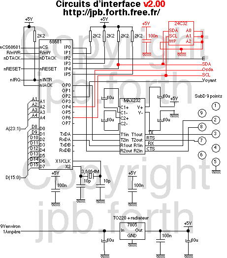
The 68681 is maybe the constituent the most difficult to
get itself. It is made by RTC ( PHILIPS) and by MOTOROLA in second
source. It has the enormous advantage to contain a programmable
timer (indispensable for the real-time kernel) and 2 serial asynchronous
links ( UART) more some ports of input - output for possible extensions.
A seeing (light electroluminescent diode) allows to realize the
activity of the processor.
A link I2C allows the use of compatible
ring peripherals and the addition of a serial EEPROM puts to protec
applications to work in a autonomous way without use of the computer
host. This EEPROM can be of type 24C32 , 24C64 , 24C128, 24C256,
or 24C512 according to the size of the application software (4
to 64 KiloBytes).
The following figures represent the electric scematic of
the card:
|
Click schematics to obtain from it an increase
|
|
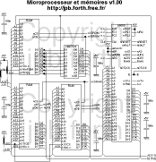
Microprocessor and memories
|
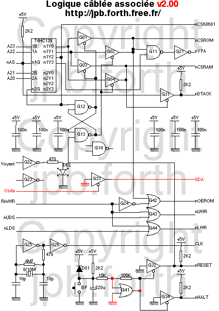
Associated wired logic
|
Circuits of interface
|
|

|

|
The position of switches S01 and S02 depend on the type
of ROM:
|
S01
|
S02
|
Type of ROM
|
|
+5V
|
+5V
|
27.128 (16 KiloBytes)
|
|
A14
|
+5V
|
27.256 (32 KiloBytes)
|
|
A14
|
A15
|
27.512 (64 KiloBytes)
|
The position of the switch S03 depend on the type of static
RAM:
|
S03
|
Type of static RAM
|
|
+5V
|
2x128Kx8 (256 KiloBytes)
|
|
A18
|
2x512Kx8 (1 MégaBytes)
|
Wired logic assures the addresses decoding for the selection
of the various chips but also a device of permutation of the RAM
selection signals and ROM. This device allows the processor to
start from the program contained in the ROM on the action of the
nRESET signal then, when its contents are downloaded in RAM, to
use exclusively this last one to benefit from the maximum of performances
(drank by data 16 bits instead of 8 bits for the ROM). The quartz
oscillator requires the use of one 74HC04 or 74AC04 with the exception
of quite other family (LS, HCT, ACT).
The DB9 connector for the link RS232 is a male connector.
A female connector can be used on the condition of crossing among
them signals RX-TX and RTS-CTS.
Power supply can be assured by means of a block transformer
supplying with a current of 1 ampere under 8 volts. Does not omi
to equip the regulator 5 volts with a heat sink allowing to dissipate
a power of 4 watts.
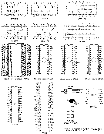
To facilitate the realization of the card, here is the pinouts of the various chips:
Click picture to obtain from it an increase
The documentation of constituents 68000 and 68681 is available
on the site www.motorola.com
from the making with the same name.