Technical pages
VGA interface
Version 1.0 of March 23, 2003
Written by jpb.forth
Timings
Definition of commands
Initialization
VGA DAC and adaptations
Introduction
These specifications describe an 480 lines of 640 pixels
VGA interface fate to be integrated into the FPGA containing the
FORTH core by using 3/4
of an additional static RAM of 512 KiloBytes and an economic 8
bits digital to analog converter allowing to show up to 256 colours.
A single register ( 16 bits) is intended to be accommodated
in the zone of extension of the heart FORTH. This register gives
access to a pile of command of VGA interface which becomes so
an internal peripheral of this processor.
Here is the synoptic plan of the VGA interface:


Timings
The 25 MegaHertz clock of the processor
is used as pixel time unit. The VGA frame is in refreshed with
a 60 Hertz frequency and cut in 525 lines. Frequency lines is
so 31,5 KiloHertz.
A simple calculation allows to determine
the total clock cycles number by line to 25 MHz are 25000000/31500
= 794 (after roundness).
The various timings can be defined
in the following way:

The signals of synchronization line and frame are negative
(0 during the duration of the pulse).
Definition of commands
The 512 KiloBytes memory is defined
as a screen of 512 lines of 768 pixels. Only a part (480 lines
of 640 pixels) is shown.
The set of registers is accessible
by transmission of commands in a first in/first out 16 bits stack
visible as a single register since the processor. VGA interface
acts then as a processor executing the present commands in the
stack.
Here is the size of this register:
Data bus
|
D15
|
D14
|
D13
|
D12
|
D11
|
D10
|
D9
|
D8
|
D7
|
D6
|
D5
|
D4
|
D3
|
D2
|
D1
|
D0
|
Write access
|
c15
|
c14
|
c13
|
c12
|
c11
|
c10
|
c9
|
c8
|
c7
|
c6
|
c5
|
c4
|
c3
|
c2
|
c1
|
c0
|
Bits c15 in c0 correspond with command.
Read access
|
C
|
L
|
0
|
0
|
0
|
0
|
0
|
0
|
p7
|
p6
|
p5
|
p4
|
p3
|
p2
|
p1
|
p0
|
Bit C indicates when it is 1 that the command stack
is full.
Bit L indicates when it is 1 that the point p7 in
p0 is valid (reading stack).
Commands are described in the following
table:
| Command |
Description |
| 00iiinnnpppppppp |
Execution of nnn time(s) the writing of the
point pppppppp to the place pointed by (X, Y) which is every
time modified according to the post incrementation mode iii |
| 01iii001******** |
Execution of the reading of the point to the
place pointed by (X, Y) which is every time modified according
to the post incrementation mode iii |
| 100000xxxxxxxxxx |
Load of the abscissa register with the value
xxxxxxxxxx |
| 100010xxxxxxxxxx |
Addition of the value xxxxxxxxxx in the abscissa
register |
| 1100000yyyyyyyyy |
Load of the ordered register with the value
yyyyyyyyy |
| 1100100yyyyyyyyy |
Addition of the value yyyyyyyyy in the ordered
register |
Here is the definition of various codes used in the commands
table:
| Code |
Value |
Description |
| iii |
0 |
(X,Y) --> (X+1,Y) |
|
1 |
(X,Y) --> (X+1,Y+1) |
|
2 |
(X,Y) --> (X,Y+1) |
|
3 |
(X,Y) --> (X-1,Y+1) |
|
4 |
(X,Y) --> (X-1,Y) |
|
5 |
(X,Y) --> (X-1,Y-1) |
|
6 |
(X,Y) --> (X,Y-1) |
|
7 |
(X,Y) --> (X+1,Y-1) |
| nnn |
0 to 7 |
Number of iterations of the action (0 corresponds
to 8 iterations) |
| pppppppp |
0 to 255 |
Code of the colour of a pixel:
- p7 corresponds to R3
- p6 corresponds to R2
- p5 corresponds to V3
- p4 corresponds to V2
- p3 corresponds to B3
- p2 corresponds to B2
- p1 corresponds to G1
- p0 corresponds to G0
|
| xxxxxxxxxx |
0 to 1023 |
Coding of the abscissa value |
| yyyyyyyyy |
0 to 511 |
Coding of the ordered value |
Registers X and Y allow of point a pixel ( a byte) of the
total image (RAM). X varies from 0 to 767 (column) and Y varies
from 0 in 511 (line).
The 8 other registers allow to reach the pixel pointed by
(X, Y) with the choice of the neighboring pixel (post incrementation
or post decrementation of X or of Y) for the following access.
This is another help in the software for various graphic subroutines.
R3 , R2 corresponds to the 2 master significant bits of
the red colour. V3 , V2 corresponds to the 2 master significan
bits of the green colour. B3 , B2 corresponds to the 2 master
significant bits of the blue colour. G1,G0 corresponds to the
2 less significant bits of the 3 colours.
Initialization
When the RESET signal is applied to the interface, registers
X and Y are set to zero.
VGA DAC and adaptations
Here is the plan of the triple digital to analog converter
(DAC) for 3 colours red, green and blue as well as the other necessary
adaptations for the VGA monitor driving:
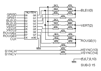
The convertion resistances values are calculated by considering
that the 74LVT574 is powored with 3.3 volts and a 75 ohms load
of on each of the input red, green and blue of the VGA monitor.
Every colour can so have 16 nuances corresponding to the voltages
of the following table:
| R3/V3/B3 |
R2/V2/B2 |
G1 |
G0 |
Output voltages in Volts |
| 0 |
0 |
0 |
0 |
0 |
| 0 |
0 |
0 |
1 |
0.051 |
| 0 |
0 |
1 |
0 |
0.101 |
| 0 |
0 |
1 |
1 |
0.152 |
| 0 |
1 |
0 |
0 |
0.203 |
| 0 |
1 |
0 |
1 |
0.253 |
| 0 |
1 |
1 |
0 |
0.304 |
| 0 |
1 |
1 |
1 |
0.36 |
| 1 |
0 |
0 |
0 |
0.41 |
| 1 |
0 |
0
|
1
|
0.46
|
| 1 |
0 |
1
|
0
|
0.51
|
| 1 |
0 |
1
|
1
|
0.56
|
| 1 |
1 |
0
|
0
|
0.61
|
| 1 |
1 |
0
|
1
|
0.66
|
| 1 |
1 |
1
|
0
|
0.71
|
| 1 |
1 |
1
|
1
|
0.76
|
This corresponds well to 16 nuances by tint but as the 2
less significant bits (G1 and G0) are common in 3 colours, one
obtains so only 256 different tints at most (4R*4V*4B*4G). This
device remains on the other hand very economic and easily practicable.
A much more important number of nuances can be emulated
by framage as shows it following example:


